ProbeAce Co., Ltd., founded in 1999, has been researching a unique and novel methodology for realizing a next-generation probe card.
The semiconductor industry has been eager for a next-generation probe card for more than 10 years. However, a conclusive method has not been realized in spite of an urgent issue. In order to develop the advanced probe card, ProbeAce has proposed a new design method, termed as the AMMECS (Advanced Micro-Mechanical・Electrical・Chemical System).
Several problems were encountered in developing the next-generation probe card. Simply using down-sizing technology for the probe card could not solve all of the technical and economic problems, such as application to parallel tests on a wafer, higher pin counts with finer pad pitch, and a probe structure that does not require tip cleaning. As another important issue, it was necessary to realize a next-generation dense probe card in a restricted small space, while maintaining the basic electrical characteristics and maintainability of conventional probe cards.
This new method, “AMMECS,” is a combination of a probe unit architecture called “Gun-Kimo Probe,” which provides a solution of fine-pitch probe arrangements for testing 2.5D/3D ICs with TSV stacking and parallelism of high-end ICs, and “Gun-Kimo Card,” which provides a solution for dense and multi-layered wiring problems.
Combining breakthroughs in precision probe technology and interconnect technology, as well as wiring technology, our AMMECS probe cards can provide a number of benefits that are unattainable in the conventional probe cards. We are confident that simultaneous solution of probe unit and wiring is the only way to provide the drastic solution for the next generation probe card.
In addition, drastic design and manufacturing automation is also one of our R&D policies. We have always been researching automated facilities while being associated with the probe architecture. By implementing automatic design and manufacturing processes, ProbeAce has the capability to offer quick turnaround to the market.
ProbeAce technology will provide total advantages for Cost of Ownership to customers, as well as probe performance.
社長挨拶
株式会社プロブエースは、1999年の設立以来、次世代のプローブカードを実現するための独自で斬新な方法論を追及してまいりました。
次世代用プローブカードの必要性は、10年以上前から半導体業界で求められてきましたが、緊急課題であるにもかかわらず決定的な方法論が見出せないままでした。このAdvanced Probe Cardを実現するため、プロブエースは新たな方法論を提唱し、これをAMMECS(Advanced Micro-Mechanical・Electrical・Chemical・System)と命名しました。
次世代用プローブカードを開発する上で幾つかの問題点が存在していました。技術課題である半導体ウェハの複数デバイス同時検査化、さらなる狭ピッチかつ多端子化、そしてプローブ先端のクリーニングレス化への適用といったような、単純にプローブカードのダウンサイジング化では解決できない技術的・経済的課題が多いことでありました。さらに重要なことは、従来型のプローブカードで実績のある電気的特性やメンテナンス性を基本的に維持しながら、小空間において高密度な次世代型プローブカードを実現しなければならないことでした。
この新しい方法論であるAMMECSは、2.5D/3D TSVや高機能ICの検査に適用可能な狭ピッチプローブ配列のソリューションを提供するプローブユニット構造としての”Gun-Kimo Probe”と、高密度・多層配線に対するソリューションを提供する”Gun-Kimo Card”から構成されます。
精密プローブ技術と、配線技術に加えてコネクション技術におけるブレークスルーを結合させることにより、AMMECSプローブカードは、従来品では困難であった多くの利益を供給できます。我々は、プローブヘッド構造上の問題と配線構造上の問題の同時解決なくしては、次世代プローブカードの抜本的解決はあり得ないと考えております。
さらに、設計製造の自動化は、我々の開発ポリシーの一つです。我々は常に、自動化装置をプローブ構造との関連付けにより開発してまいりました。自動化された設計及製造工程の導入によって、プロブエースは市場に短納期化を提供する能力を有しております。
プロブエースの技術は、優れたプローブカード特性はもちろんのこと、ユーザ保有コスト低減にも貢献し得る総合的な技術を目指しております。
実際どこがそんなに凄いのか分からないと言う方へ
下記アドレスに「会社名・ご所属・ご氏名」等を記載の上、資料をご請求ください。弊社より返信メールにてお送りいたします。
Email: information@probeace.co.jp
Profile of President Kimoto
History
1965 Entered NEC Corporation and engaged in mechanical engineering field; Printers, Automation facilities, Robots etc.
1972 Invented and completed the Japan’s first dot impact Kanji printer, published in the Information Processing Society of Japan (IPSJ) vol.45 No.1 2004.
1999 Established ProbeAce and installed as director. Started development of probe card.
2008 Installed as president of ProbeAce.
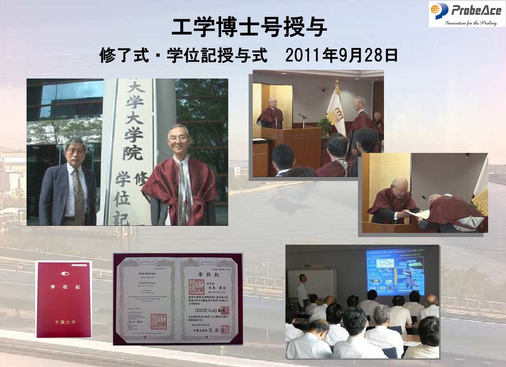
2011 Awarded the degree of Doctor (Mechanical engineering) from Chiba University.
Papers (as a first author)
“Contact probe card with large overdrive,” Electro Chemical Society Transactions, vol. 33, pp57-67, 2010.
“A new contact probe without cleaning process,” Transaction of Japan Institute of Electronics Packaging vol. 3, No. 1, 2010.
“New development of contact probe and methodology,” Advanced Materials Research, vol. 126-128, pp 726-731, 2010.
“Design and Manufacture of Novel Probe Card for Testing 3D ICs with TSVs,” IEEE EPTC2012.
“Novel Probe Card with High Count of Needles in Single Sheet for Universal Wafer Testing,” IEEE SWTW2013.