New information
ProbeAce New Solution for 3D/2.5D IC-Interconnect Technology published, 23 Sept. 2021 >>> Go to the page
ProbeAce Co.,Ltd. provides a new solution for non-silicon process IC-interconnect technology, which can replace the current methods of, e.g. “3D-IC integration with TSV” and “2.5D-IC integration with silicon interposers/bridges” with lower cost. Especially in the 3D-IC integration, this method will enable various type of heterogeneous IC-interconnect design flexibly, because of no restrictions on process-node, wafer size, die/package size, and I/O layout.
プロブエースの「ICインターコネクト技術に関する新ソリューション」を公開しました。2021年9月23日→ Go to the page
株式会社プロブエース(http://probeace.co.jp)は、従来の例えば「TSVによる3D-IC実装」及び「シリコンインターポーザ等による2.5D-IC実装」を低コストで代替可能とする、非シリコンプロセスによるICインターコネクト技術に関する新たなソリューションを提供します。特に3D-IC積層分野では、本方式により、プロセスノード、ウェハサイズ、チップ又はパッケージサイズ、端子配列等の制約無く、様々な異種混合ICを柔軟に組合せることができます。
19 March 2019, ProbeAce (PA) signs a Memorandum Of Understanding (MOU) with aps Solutions GmbH (APS) , located in Munich, for exclusive Distribution of PA’s contactor technologies in EU and Israel. >>> Go to Media
2019年3月19日に当社は、ドイツミュンヘンに本社を置くaps Solutions GmbH社と、EUとIsrael市場における当社が有するチップコンタクト技術の独占販売店契約に関するMOUにサインした。→Media 参照
All about Test – Latest Test and Measurement News
aps Solutions sells Chip contacting Technology of ProbeAce in Europe and Israel
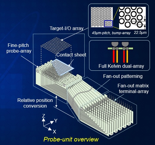
19 March 2019 – aps Solutions GmbH (APS) announced signing a Memorandum Of Understanding (MOU) with ProbeACE (PA), an innovative Japanese Probe Card manufacturer, for exclusive Distribution of PA’s contactor technologies in EU and Israel. ProbeAce recently announced their “Fine-Pitch Area-Array Probe-Unit”, a Contactor solution, which is focusing on the increasing market of IoT (Internet of Things) devices as the versatile multi-connection technology as well as FOWLP (Fan-Out Wafer Level Package) package testing.
ProbeAce has succeeded in developing a new Probe Card opening up a new era of wafer level package. ProbeAce has achieved drastic cost reduction on high-performance Probe Cards with new design and manufacturing methods, characterized by a film-shaped probe-and-wire integrated sheet structures in response to increasing demand of cost effective contacting solutions.
To expand the pitch between pins from the wafer-level fine-pitch in the densification area (the Probe Head) to the wider Probe Card PCB technology pitch, ProbeAce uses a proprietary monolithic manufacturing method. Fan-out patterns are seamless formed continuously from each probe to optional test area without any high
cost space-transformers/interposers generally used in current probe cards. This characteristic nondiscontinuous fan-out pattern structure reduces reflection losses; furthermore designing impedance-matching structures along the signal lines enables superb electrical performance also for RF applications.
Dr. Gunsei Kimoto, President of ProbeAce stated: “With this innovative method, massive probe and fan-out patterns were designed and manufactured significantly cheaper and faster. We have developed a 22.5-um pitch and 30,000-pins-class area-array probe-unit with non-discontinuous fan-out structure without interposer substrates using the monolithic fabrication method and demonstrated the high precision probe array and high
productivity.”
“I’m impressed about ProbeAce’ technology for the Semiconductor wafer test, which we now can provide to our customers in Europe and Israel. Working for more than 25 years as Production Manager in large wafer test sites, I was faced with the increasing costs and interfacing complexity of high pin-count and high parallelism Probe Cards as a consumable product for the wafer test – the ProbeAce approach might be a “Game Changer””, said Hanns-Georg Ochsenkuehn, Managing Director of APS.
apsはProbeAce保有のチップコンタクト技術をEUとIsrael市場において販売する。
2019年3月19日― aps Solutions (APS)は、ProbeAce(PA)(日本の革新的プローブカード製造メーカ)とEUとIsraelにおけるPAのコンタクタ技術に関する独占販売店についてのMOUにサインしたことを発表した。ProbeAceは最近、”Fine-Pitch Area-Array Probe-Unit”と称するコンタクタソリューションを発表した。これは、益々増加するIoTデバイス市場におけるコンタクタの課題に焦点を当てたものであり、FOWLP (Fan-Out Wafer Level Package)の他、汎用的なマルチコネクション技術に適用するものである。
ProbeAceは、ウェハレベルパッケージの新時代を切り開く新しいプローブカードの開発に成功した。ProbeAceは、高機能プローブカードの抜本的なコスト低減を新しい設計製造方式により達成した。これは、フィルム型プローブ/配線一体シート構造に特徴づけられ、低コストのコンタクトソリューション要求の増加に対応している。
高密度領域(プローブヘッド)におけるウェハレベルの狭ピッチから、プローブカードPCB技術のピッチまでピン間ピッチを広げるため、ProbeAceは独自の一体化製造方式を使用した。各プローブから選択されたテスト領域までを、現行のプローブカードで一般的に使用されている高コストのスペーストランスフォーマー/インターポーザを使用することなく、fan-outパターンがシームレスに形成されている。この特長的な連続的fan-outパターンは反射損失を低減し、さらに、信号ラインに沿ってインピーダンス整合構造に設計することにより良好な電気的特性を可能とし、高周波に適用できるものである。
木本軍生Dr.(ProbeAce代表)は、「この革新的方式により、大量のプローブとfan-outパターンがより安く早く設計製造される。我々は、インターポーザ基板を使用することなく、一体化製造技術を使用した連続的なfan-out構造により、22.5umピッチ、30000ピンクラスのエリアアレイプローブユニットを開発し、高精度プローブアレイと高い製造性を実証した。」と述べている。
「私は、EUとIsraelの我々の顧客に供給できるこの半導体ウェハテストのためのProbeAce技術に感動した。ウェハテストにおけるプロダクションマネージャとして25年以上携わり、ウェハテストの消耗品としてのプローブカードにおいて、多ピン化と複数テスト化の増大するコストとインターフェースの複雑化に直面してきた。ProbeAceのアプローチは、“Game Changer”となるかもしれない。」とHanns-Georg Ochsenkuehn, Managing Director of APSは述べている。
Our new technology and products “Fine-pitch Area-array Probe-unit” is now published in the SWTest Asia 2018.
“A High-density Area-array Probe-unit with Non-discontinuous Fan-out Structure without Space Transformer using Monolithic Fabrication Method”
ProbeAce current status
Since establishment in 1999, ProbeAce has been developing and accumulating the patented technology as the world-top-class “Fine-pitch multi-I/O connection technology”, starting with the probe card technology used in the semiconductor wafer test. Our technology can widely expand to the IoT market as the versatile multi-connection technologies, as well as FOWLP*1) in the semiconductor fields. This capability is because its versatility, applicability to the future demand, and cost-effectiveness, which other companies do not have and cannot catch up with.
*1) Fan-Out Wafer Level Package
Why does the world need “ProbeAce” now?
Keywords of the Fourth Industrial Revolution are “IoT” and “AI”. As discussing at a tangible electrical circuit layer, the market needs a means that a large mass of information can be transmitted at high speed freely in three-dimensional space, adding the condition that related products can be designed and manufactured cheaper and faster.
ProbeAce is now located under urgent situation in the market because that the time has come for us to propose our prototype products. We have received a request to present a paper from an academic conference, and some inquiries and requests to produce concrete prototypes from many world-class companies. Only ProbeAce technology can meet above conditions in the world. It has been demonstrated in the following that we received orders of the next-generation circuit products from some leading companies. Our unique technology has been protected by original patents. It will be so dangerous for competitors to imitate our patented technologies. No solution exists on a conventional extension line.
当社は1999年の設立以来、半導体製造工程のウェハ検査に使用される「プローブカード」技術の開発と共に、世界トップクラスの「狭ピッチ多端子接続技術」としての特許技術を蓄積してきた。我々の技術は、FOWLPを代表とする半導体分野での適用だけでなく、多目的の多端子接続技術にも広く適用可能であり、今後のIoT市場において大きく進展する技術である。これは、他社が現有せず、かつ追従できないほどの当社技術の持つ汎用性、将来性、そして低コスト実現性によるためである。
何故今この時にプロブエースなのか?
第4次産業革命のKeyワードが「AI」であり「IoT」である。これを実際の電子回路で言うならば、市場は、3次元空間内において自由に大量の情報が高速に通信可能となる手段を必要としている。更には、関連する製品が安く・早く設計製造できることの条件付きである。
我々の現在置かれている状況は緊迫している。上記電子回路の試作商品提起する時期が到来しているからである。現在、当社は学会からの発表と世界を代表する企業からの問い合わせと具体化試作に、その対応が求められている。上記条件をクリア出来る企業は唯一プロブエースになると考えている。次世代の回路製品が有力企業から既に発注されていることが、それを証明している。この技術は既に独自の特許でガードされている。他社が真似るには相当の覚悟が必要である。従来技術の延長線上では解決策は存在しない。