Our Probe Card Technology
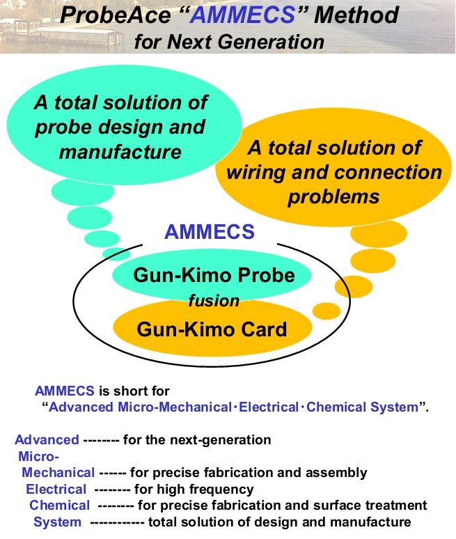
Since founded in 1999, ProbeAce has been researching a unique and novel methodology for realizing a next-generation probe card. The semiconductor industry has been eager for a next-generation probe card for more than 10 years. However, a conclusive method has not been realized in spite of an urgent issue. In order to develop the advanced probe card, ProbeAce has proposed a new design method, termed as the AMMECS (Advanced Micro-Mechanical・Electrical・Chemical System).
Background of probe card technology and test market
A probe card is an interface between a semiconductor wafer and an electronic test system. The probe card is put into equipment called a wafer prober, inside which the position of the wafer to be tested is manipulated so that there is a precise contact between each probe tip and I/O pad on the wafer.
While the rapid progress of scaling and highly integration including 3D/TSV, conventional probe card technology has already reached the limit of its array pitch and configuration. There is no single method covering the wide range of probe card technologies in the marketplace as stated in the ITRS, so leading different technologies such as “cantilever type,” “vertical type,” and “MEMS type” is shared depending on the test categories. Probe card structure is constantly becoming more complicated in the progress of device scaling and highly integration, so the interface cost including probe cards will be also increasing year by year.
Probe card technologies are facing complex electrical, mechanical, and economical challenges driven by product specifications, test requirements, and reduced test cost demands. Research and development of cost effective probe card technologies is urgently required to meet the rapid progress and variety of test applications in the semiconductor industry.
Features and Advantages of Our Probe Cards
Our new method, “AMMECS,” is a combination of a probe unit architecture called “Gun-Kimo Probe,” which provides a solution for fine-pitch probe arrangements for testing 2.5D/3D ICs with TSV stacking and parallelism of high-end ICs, and “Gun-Kimo Card,” which provides a solution for dense and multi-layered wiring problems. Combining breakthroughs in precision probe technology and interconnect technology, as well as wiring technology, our AMMECS probe cards can provide a number of benefits that are unattainable in the conventional probe cards. We introduce a wide variety of following solutions:
1. High-pin-count and fine-pitch needles in a single sheet
This method is our basic probe architecture, which is a set of hundreds of contact needles and terminals fabricated by laser processing, using a heat-treated Be-Cu thin material. In many conventional cases, each probe needle is hand built by highly skilled technician. In contrast, we achieved the method that is free from conventional “a-needle-as-a-part” manufacturing and manual assembly like cantilever probe, in other words, simultaneous process of massive needle fabrication and precision assembly for a row of I/O pads.
This sheet-structural probe has a compatibility with batch-process of multi-needles, patterning to circuits and insulation coating, and easiness to compose a multi-layered probe patterning with ground layers for high frequency, for example, impedance-matching probe sheet with strip-line or micro-strip-line structure, and probe sheet with guard structure for low leakage current.
2. Precise Tip Motion Parameter Controllable Structure
Three important probe-tip motion parameters are “contact force,” “overdrive” and “scrub motion” to determine probe contact characteristics. It is very important to design an optimal set of these three parameters for probing certain device types. But in case of cantilever probe, the three parameters are determined depending on its probe arm design. A basic cantilever form design of a horizontal long beam and vertical needle makes a correlation among these three parameters. So the resulting excessive contact force or scrub motion leads to a die damage or contamination from pads/bumps.
Our probes are produced by 2D laser process of a thin Be-Cu film, which enables any complicated curves to meet optimal probe shape. So we can set up each parameter independently. This probe technology provides following advantages:
- Small or non-scrub motion with large overdrive design for small-area and ultra-fine pitch pad/bump,
- Small or non-scrub motion design for contamination-free probing preventing online tip-cleaning,
- More than 100 um large overdrive for large area probing of 300-450mm wafer contact.
3. A Combination of Probe Sheets meets Universal Assembly
Recent semiconductor market trend, such as highly integration and scaling of device, parallelism, and 3D-stacked ICs, increases the number of I/O pads for testing and makes pad arrangement more complicated. The number of pads and the pad arrangements influence probe arrangements.
For example, memory ICs generally have simple dual line pad arrangements, though it requires entire simultaneous die testing on a wafer. This necessitates a high-pin-count probe design with several tens of thousands of pins. On the other hand, LCD driver ICs have more precise pad arrangements as a number of pixels increase, and it has a very fine pitch of less than 15 um as well as a small pad size. Furthermore, to enable more functionality in smaller packages, manufacture trend is moving toward 3D-stacked ICs with TSV technology. Ultra-fine-pitch area array probes of less than 50 um are required for direct TSV probing.
However, nowadays, there is no single probe technology to meet a wide variety of pad arrays. Using our method, a certain row is composed by multi-probe needles in a single sheet, and columns are composed by multiple probe sheets arranged repeatedly in parallel. So the basic architecture of our probe head assembly is fine-pitch area-array. And this basic architecture has extensibility to fine-pitch peripheral or parallelism.
This probe technology meets a wide variety of geometrical requirements across the entire device category with a single manufacturing method.
当社のプローブカード技術
株式会社プロブエースは、1999年の設立以来、次世代のプローブカードを実現するための独自で斬新な方法論を追及してまいりました。次世代用プローブカードの必要性は、10年以上前から半導体業界で求められてきましたが、緊急課題であるにもかかわらず決定的な方法論が見出せないままでした。このAdvanced Probe Cardを実現するため、プロブエースは新たな方法論を提唱し、これをAMMECS(Advanced Micro-Mechanical・Electrical・Chemical・System)と命名しました。
プローブカード技術及びテスト市場の背景
プローブカードは、プローバ装置に搭載され、半導体ウェハ製造工程における電気的検査工程に使用されます。ウェハ上の半導体の微小な電気端子(パッド)と検査装置(テスタ)とのインタフェース機能を有し、狭ピッチかつ多数の針(プローブ)を搭載した配線基板です。
従来のプローブカード技術は、配線の微細化、TSVによる三次元実装化を含む異種混合による多機能集積化といった半導体製造技術の急激な進歩に対し、プローブピッチ及びプローブ配列形状の面ですでに物理的限界に達しています。また、ITRSが指摘しているように、一つの技術で市場にあるプローブカード技術を広くカバーできる方法論が存在していません。そのため、対象となる検査カテゴリごとに「カンチレバー型」「垂直ピン型」「MEMS型」といった異なるプローブ設計及び製造方式によるものを使い分けているのが現状です。縮小化・多機能集積化の一途を辿る半導体の検査分野においてプローブカードの構造はますます複雑なものとなり、プローブカードを含むインタフェースコストも年々ますます上昇することでしょう。
プローブカード技術は、製品仕様やテスト要求、そしてコスト削減の要求などに左右される複雑な電気的、機械的そして経済的な課題に直面しています。半導体製造分野における急激な進歩と多種にわたる検査アプリケーションに追従する、低コストのプローブカード開発が早急に求められています。
当社プローブカードの特徴と優位性
我々の新しい方法論であるAMMECSは、2.5D/3D TSVや高機能ICの検査に適用可能な狭ピッチプローブ配列のソリューションを提供するプローブユニット構造としての”Gun-Kimo Probe”と、高密度・多層配線に対するソリューションを提供する”Gun-Kimo Card”から構成されます。精密プローブ技術と、配線技術に加えてコネクション技術におけるブレークスルーを結合させることにより、AMMECSプローブカードは、従来品では困難であった多くの利益を供給できます。以下に、様々なソリューションをご紹介します。
1.多数のプローブを一括搭載するプローブシート方式
この方式は、数百ものプローブ針と接続端子からなる我々のプローブ構造の基本となるもので、熱処理済Be-Cu(ベリリルム銅)箔をレーザ加工することにより製造されます。従来から多くの場合、一つ一つのプローブは高度に熟練した技能者によって手で組立てられます。我々の本方式により、従来のカンチレバー型プローブのような「1プローブ1パーツ」製造方式及びマニュアル組立からの脱却を実現しました。言い換えれば、1列分のI/Oパッド相当の針製造と高精度組立が同時工程で実現されることになります。
このシート型プローブ構造とすることにより、多ピン加工・接続配線・絶縁処理の一括製造が容易になり、また、プローブパターンとグランド層との多層化も容易であるため、ストリップラインやマイクロストリップラインといった高周波用パターンを構成することが出来ます。さらに、ガード構造とすることにより、低リーク電流のためのプローブシートを実現することが出来ます。
2.先端動作パラメータのコントロール可能なプローブ構造
プローブ先端動作における3つの重要なパラメータは、接触力、オーバードライブ、スクラブであり、これらによりプローブのコンタクト特性が決定づけられます。これらの3つのパラメータを検査対象ICごとに最適化することは、種々のデバイスをプロービングするために非常に重要な設計要因です。ところが、カンチレバーでは、そのプローブ形状によって3つのパラメータの関係が決定されてしまいます。すなわち、基本的なカンチレバー形状である長い水平方向梁と垂直針の関係が、3つのパラメータ間の相互依存を作ってしまいます。その結果生じる過剰な接触力やスクラブ動作は、ICへのダメージやゴミの発生を引き起こします。
我々のプローブは、最適なプローブ形状を実現する複雑形状加工を可能とするBe-Cu箔の二次元レーザ加工によって作られます。従って、各パラメータを独立に決定することが出来ます。このプローブ技術によって、次のような優位性のあるプローブを提供します。
- 狭小・狭ピッチパッドに適応可能な、十分なオーバードライブでの極小又はノンスクラブ動作
- 先端クリーニングを不要とする、ゴミを発生しない極小又はノンスクラブプローブ動作
- 300 mm又は450 mm径ウェハコンタクト等の広域プロービングに適した、100 um超の大オーバードライブ
3.あらゆるパッド配列に対応可能なプローブシート方式
今日における半導体市場のトレンドとして、デバイスの高機能化と縮小化、複数デバイス同時測定、三次元集積化等があります。こうしたトレンドはテスト用I/Oパッドの増加と配列の複雑化をますます牽引しています。テストパッドの数と配列は、プローブ配列に大きく影響します。
例えばメモリICでは、一般的にシンプルな直線配列パッドですが、ウェハ上での多くのチップの同時測定が要求されます。この測定のためには、数万ピンも搭載したプローブカードが必要となります。一方、液晶画面駆動用ICでは、画素数の増加に伴いより精密なパッド配列となり、パッド面積の縮小化と共に15umを下回る狭ピッチな配列が要求されます。また、小パッケージ下でのさらなる高機能化のために、半導体製造のトレンドは確実にTSV技術を用いた三次元積層組立の方向に向かっています。TSVへの直接プロービングのためには、50 umピッチを下回るエリア配列プローブが要求されます。
ところが今日、一つのプローブ技術で多種多様に存在するデバイスのパッド配列を満たすものは存在しません。我々の方式によれば、一つの列はプローブシート製造により、直交する他の列はプローブシートの平行配置によって構成されます。従って、我々のプローブヘッドの基本形状は狭ピッチの格子配列であるといえます。この基本形状からさらに、狭ピッチ周辺配列又はパラレルテスト配列へ拡張することが出来ます。
このように、このプローブ技術によれば、一つのプローブ製造技術ですべてのデバイス群の非常に多くの配列要求を満たすことができます。