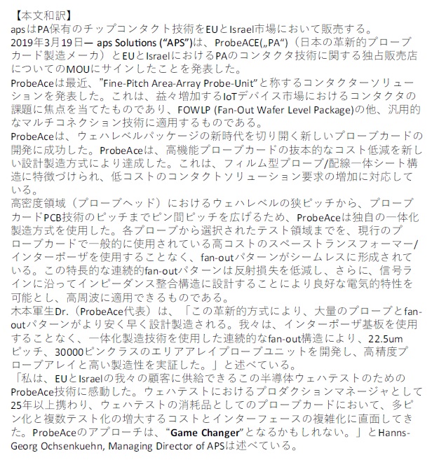
New information from aps Solutions GmbH (APS) , Munich
All about Test – Latest Test and Measurement News
President Interview: Electronic Device Industry News, 5th May 2018
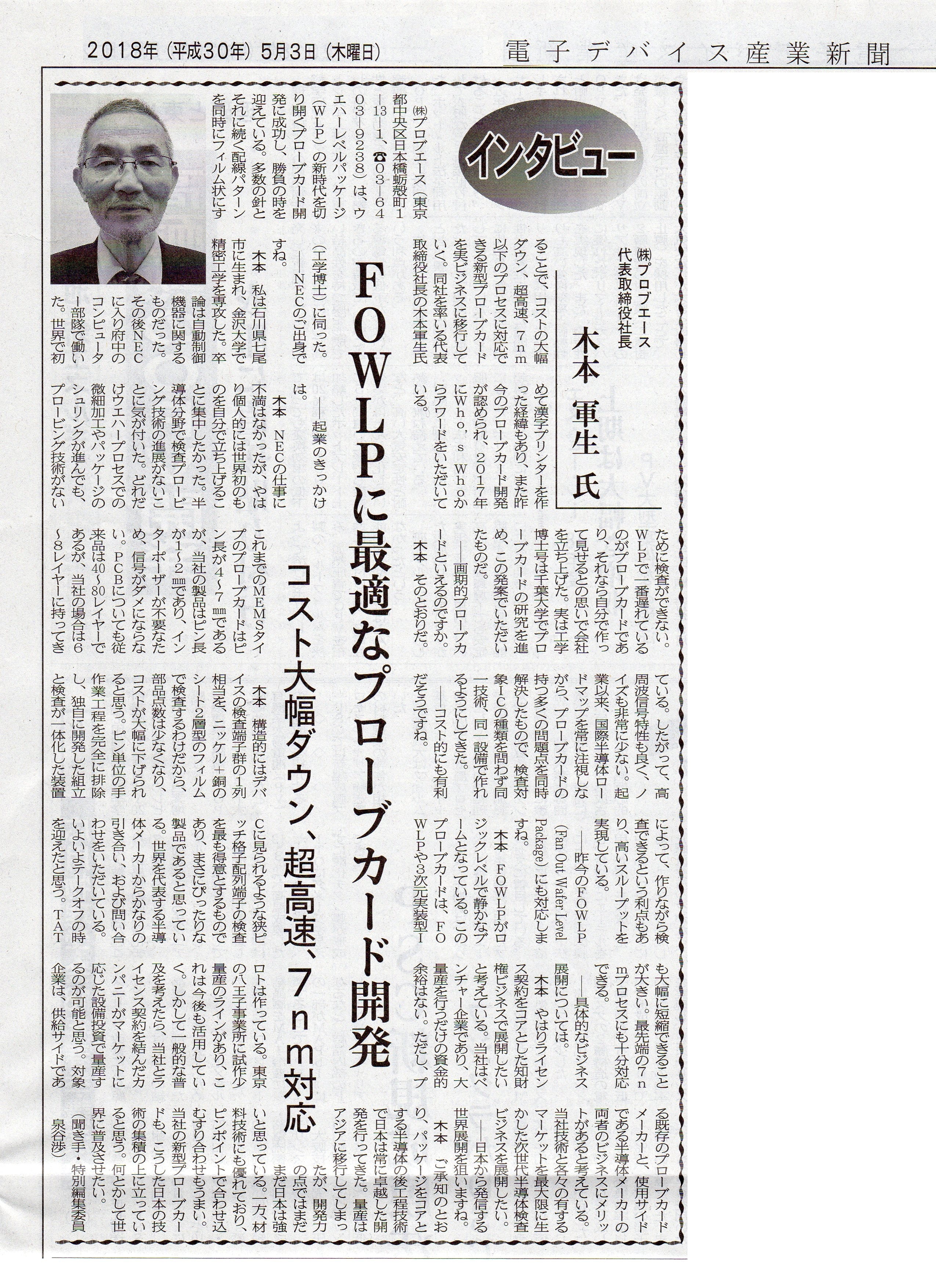
ProbeAce, (1-13-1-B1 Nihonbashi Kakigara-cho, Chuo-ku, Tokyo 103-0014, Phone: +81-3-6403-9238) has succeeded in developing the new probe card opening up a new era of wafer level package. ProbeAce has achieved drastic cost reduction and high-performance probe cards with new design and manufacturing method, characterized by a film-shaped probe-and-wire integrated sheet structures in response to increasing demand. It is just now the time for entering the real market.
This is the interview to President Gunsei Kimoto, (Ph.D. in Engineering) of ProbeAce, published in the Electronic Device Industry News, on the 5th of May 2018.
Q: Have you ever involved in NEC?
A: I was born in Nanao-city, Ishikawa-prefecture, and majored in precision mechanical engineering at the Kanazawa university. My thesis was related to the automatic control equipment. After that, I entered the NEC Corporation and engaged in the computer department in the Fuchu-branch. I was awarded the Marquis Who’s Who “Albert Nelson Marquis Lifetime Achievement Award” in 2017, in recognition of my achievement rerated to the recent probe card study, as well as my history of invention of the world’s first “Dot-impact Kanji printer” in 1972.
Q: Well, what made you start-up?
A: It’s never from dissatisfaction in NEC, of course. Personally, I wanted to concentrate to start up by myself for the world’ first leading-edge technology that no one can catch up and imitate. I found there is no progress on test probing technology in the semiconductor field for many years. While the rapid progress of scaling and fine processing technology in wafer process, or shrinking packages, probing technology is still behind for precise and effective wafer test. Probe cards are behind especially in the device test technology using wafer level package (WLP). So, if that’s the case, I started up the company, thinking that I would surely make it by myself. That is the reason. As a matter of fact, I was awarded the degree of doctor (Mechanical engineering), as the results of the probe card research in Chiba University in 2011.
Q: We could say that is an epoch-making probe card?
A: Off course. In fact, current MEMS-type probe cards widely used in fine-pitch area array I/O tests have some problems. Our probe card has good electrical performance like high-frequency signal characteristics with lower noise, because probe pin length is only 1 to 2 mm, and fan-out wiring structure dose not depend on any multi-layer substrates, only with 6 to 8-layer PCB as a basic power/ground structure. On the other hand, MEMS-type pin length is usually 4 to 7mm, and interposers/space-transformers and high-multilayer (40 to 80 layers) PCB are inevitable for fan-out from dense probe area to rough test terminal area. Since staring-up, I always pay close attention to the trends in the International Technology Roadmap for Semiconductors (ITRS). Consequently, it has been reached that a common technology method of probe card design and manufacturing process was realized for various applications in leading semiconductor categories, including significant solutions of the difficult challenges stated in the ITRS.
Q: I heard it is also cost effective?
A: The best thing of all, the number of components were extremely reduced. I should say “non-per-pin” fabrication and assembly process were achieved. A number of pad/bump rows in the device I/O terminals can be tested with a couple of films having probe-and-wiring patterns. Dual material in a line by electroforming process will be possible. Our technology is freeing from high cost elements: high-multilayer substrates and skilled-hand process. So high through-put productivity and short TAT were achieved by collectively fine patterning design and single process of high-precision electroforming. We have also developed the in-process manufacture/test equipment in terminal-tip forming and electrical line performance test process.
Q: So, is it expected to be applied in the recent FOWLP?
A: FOWLP technology is an enhancement of standard wafer-level packages (WLPs) developed to provide a solution for semiconductor devices requiring a higher integration level and a greater number of external contacts. Our probe card is exactly good at probing fine-pitch area array bumps, like FOWLP or TSV-stacking ICs. TAT can also be significantly reduced, and it will be applicable to the cutting-edge 7-nanometer node. As results of our marketing, several large companies are fortunately paying attention to the progress of our technology. I am sure it has finally reached the time of “take-off”.
Q: Tell us about your concrete business development?
A: We are planning to make license businesses with many companies in response to increasing market demand and spreading our new technology into the market. R&D venture company like us does not have enough resource for high-volume manufacturing. But we have the process for prototype in Hachioji, Tokyo, as the base of our core technology. I think it would be better that each licensee makes investment in equipment depending on the respective size of the market. This business is advantageous for both a user and a seller, or probe card vendors as a supply-side, and fabless/foundry/test-house as a user-side. I would like to expand the next generation semiconductor test business by taking maximum advantage of the ProbeAce technologies and the market opportunities owned by each business partner.
Q: Your aim is global expansion originating from Japan?
A: That’s right. As you know, in Japan, outstanding development has always been carried out in the back-end process, especially packaging as the core technology. Mass production has shifted to Asia, but I believe Japan is still strong in terms of development power, and it is also excellent in material technology. Our new probe card technology is standing on the integration of such technologies. I would like to manage to widely spread this technology to the world.