A Highly-cost-effective Area-array Probe-unit as a Key Hardware Technology in Quality Management System for IoT Products
IoT製品のための品質管理システムの主要ハードウェア技術としての低コストエリアアレイプローブユニット
This technology is the highly-cost-effective high-density area-array probe-unit which consists of four functions, “Densification,” “Fan-out (non-discontinuous),” “Connection,” and “Transformation,” designed and manufactured by our unique monolithic fabrication method, as a key hardware technology of quality management system in a production site for the Internet of Things (IoT), Artificial Intelligence (AI), and Big Data fields. This new probe-unit provides a multiple test/monitor function with high accessibility to I/O density and a high signal integrity structure for providing test signals or collecting massive data between the semiconductors/devices and testers. And this probe-unit is widely available as a versatile interconnection system connecting directly the wafer-level fine-pitch terminals with the test/monitor terminals which is compatible with motherboard technology pitch requirements. At the same time, we have also developed the monolithic fabrication method that an entire matrix probe array with subsequent fan-out patterns and monitor terminal array was created from a single conductive film and formed only by folding like “Origami” (paper-folding). In this innovative method, massive probes and fan-out patterns were designed and manufactured significantly cheaper and faster. We have developed a 22.5-um pitch and 30000-pins-class area-array probe-unit with non-discontinuous fan-out structure without interposer substrates using the monolithic fabrication method and demonstrated the high precision probe array and high productivity.
The IoT, AI and Big Data have been important key-words in technology industry in recent years. Growing number of physical objects are being connected to the Internet by realizing the vision of the IoT. Semiconductors and devices inevitably need interrelated requirements of cost effectiveness, thinner and/or smaller form factor, high performance and integration, adding the condition of a significant increase in input/output (I/O) density.
Semiconductors are globally used in the IoT, AI and Big Data fields. The IC trend has always been shrinking die sizes with increasing I/O density, although with the demand for higher performance, so the I/O configuration must be finer-pitch and area-array (or matrix-shape) geometrically, both at the die and the advanced package level. A transition from traditional packages to fan-out wafer-level packages (FOWLP) is inevitably required to achieve maximum connection density and thinner area-array package dimensions, improved electrical and thermal performance especially in mobile markets.
As another example of I/O density, a large size display needs also massive area-array fine-pitch I/O points with several tens of thousands of pads for connecting each pixel, which works also test points for on/off display test.
The vision of IoT is to realize the interconnectivity between sensors, actuators, computers and processes. In the process of realization of each IoT, AI and Big Data products, multiple testing or massive data monitoring between the semiconductors/devices and testers are needed. Thus, we must discuss a testability of integrated devices in process. Especially for higher integration device, testing in an early stage is highly important because one defect in one integrated device can ruin the whole device. Detecting defects can save the unnecessary costs for the subsequent manufacturing steps. Therefore, a factory needs a flexible versatile interconnection system which can connect directly the wafer-level fine-pitch terminals with the test/monitor terminals compatible with motherboard technology pitch requirements in three-dimensional space freely, adding the condition that such related connection devices must be designed and manufactured cheaper and faster.
A representative connection device for silicon process technology pitch requirements is a probe card for detecting semiconductor defect in wafer-level. However, traditional and current probe card technologies are reaching their limits in terms of the performance, pin-shrinking and scalability required to meet the needs of emerging applications. Especially, the massive-pin-count fine-pitch area-array probing has long been one of the biggest challenges in the probe card field. The probing system must be easy to adjust the I/O configuration and easy to connect the test terminals, for coping with various IC technology option flexibly. A current Vertical-MEMS-type used as an area-array probe card has general features below, which are the cost factor from the perspective of cost efficiency and performance.
1) Probe pins have been traditionally independent parts and handled with highly-skilled assembling process, and per-pin maintenance becomes harder work, as a matrix density increase.
2) High-layer and high-density space-transformers or interposers are used for fan-out patterning.
3) High-layer substrates create many discontinuity points unfavorable to high frequency performance.
We have been researching and accumulating the fine-pitch multi-I/O connection technology, starting with the probe card technology for solving problems above, characterized by the sheet-like-structure probe and fan-out patterning technology. At this time, further developed new structure and manufacturing method were achieved with the following objectives and concepts:
1) Simple structure and manufacture method for high-productivity and cost-effectiveness,
2) Flexible installation or arrangement on a test board/system,
3) as well as Matching the future market requirements.
Application concept
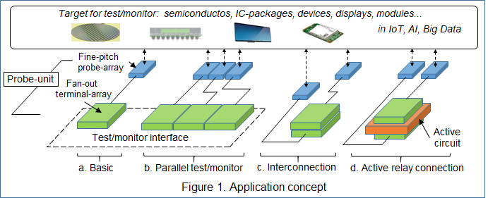
As the application concept, this probe-unit was designed with the intent to act as a key hardware device in the total quality management system in the production site for IoT, AI, Big Data Products, for achieving the versatile and cost-effective interconnection system connecting directly semiconductor-level fine-pitch terminals with the test/monitor terminals compatible with motherboard technology pitch requirements with easy handling. The application is expected to be wide-ranging. Figure 1 shows some recommended application of the probe-unit. In Figure 1, type-a is a basic application often used as a probe card for wafer/package test. Type-b shows a parallel test structure for testing multiple chips simultaneously on a wafer for the test cost reduction. In type-c, two terminal-arrays connect each other for connecting the corresponding two devices electrically. Furthermore, in type-d, an active circuit can be inserted between the two terminal-arrays for adding an active function like signal switching.
Probe-unit configuration
The highly-cost-effective high-density area array probe-unit consists of following four functions, as shown in Figure 2.
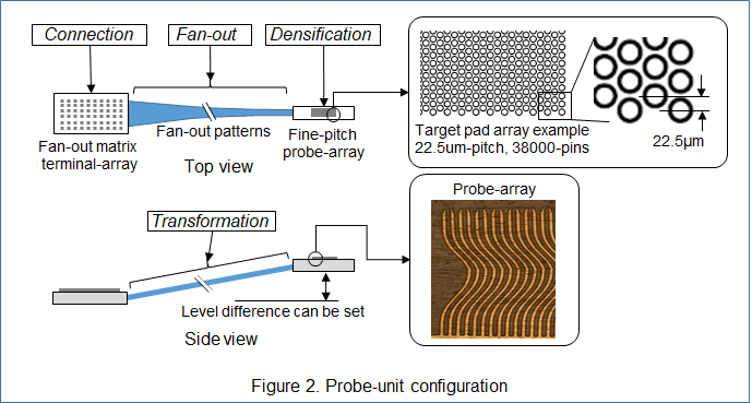
Densification. This function enables high accessibility to I/O density with wafer-level fine-pitch like IC or IC-package terminals. This part consists of probe-pin array which is accurately compatible with the relative coordinate of target device terminal array. Every probe-pin has spring characteristics independently to the target device terminals and thus can operate to contact with optimal contact forces. Since all the probe-pin of the array were formed by electroforming as an Integrated pattern, even high-pin-count (several tens of thousands of) probe-pins were formed at the same time, while Figure 2 shows the target pad/bump is 22.5 μm-pitch-array as an example.
Fan-out. Fan-out means to expand the pitch between pins from the wafer-level fine-pitch in the densification area to the wider motherboard technology pitch. Fan-out patterns were seamlessly formed continuously from each probe to optional test area without any high cost space-transformers/interposers generally used in current probe cards. This characteristic non-discontinuous fan-out pattern structure reduces reflection loss, furthermore, constructing impedance-matching structures easily formed along the signal lines enables high electrical performance.
Connection. A fan-out matrix terminal-array was formed for contacting the test/monitor terminal. This part also consists of probe-pin array which is directly connected with each probe-pin in the densification area and has also spring characteristics to easily contact with outer probes or another probe-unit.
Transformation. This function is a relative position conversion between the densification probe-array and fan-out matrix terminal-array, and thus enables flexible placement on a board or test system. The length or shape of the fan-out patterns part can be flexibly designed to match the test/monitor equipment.
Monolithic fabrication method
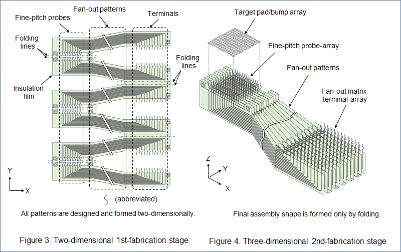
An entire probe-unit with every four functions above was created from a single conductive film in the following steps. Figure 3 and Figure 4 show the basic concept of the monolithic fabrication method.
Design-step: Entire patterns including probe shapes, fan-out patterns, terminal-probe shapes, and insulating film shapes were designed on a single X-Y coordinate plane, and thus every coordinate data were managed as an interrelated in a common coordinate, as shown in Figure 3.
1st-step: As a 1st-fabrication stage, all patterns were formed by electroforming of Nickel aminosulfonate two-dimensionally based on the common coordinate designed.
2nd-step: As a 2nd-fabrication stage, the final assembly shape was formed only by folding like “Origami” (paper-folding) three-dimensionally from the two-dimensional pattern film of 1st-step, without precision assembly process, as shown in Figure 4.
本技術は、今日及び将来のIoT分野に向けた生産現場における品質維持システムの主要ハードウェア技術として、独自の一体化製造方式によって設計製作された「高密度配列」「配線拡張(不連続点無し)」「接続」「位置変換」の4つの機能で構成される低コスト高密度エリアアレイプローブユニットについて述べたものである。
この新しいプローブユニットは、半導体又はデバイスとテスタ間でのテスト信号供給や膨大なデータ収集のための、高密度I/O端子への高接触性と高信号品質構造を有するテスト/モニタ機能を有するものである。またこのプローブユニットは、ウェーハレベルの狭ピッチ端子群とマザーボード技術におけるピッチを有するテスト/モニタ端子群とを接続する、多目的相互接続システムとして使用されるものである。
同時にまた、一体化製造方式を開発し、一連のマトリクスプローブ配列とそれに続く拡張配線及びモニタ端子配列が一枚の導電性フィルムから作製され、『折り紙』のように折り曲げのみで形成されるものである。この革新的な方式によれば、膨大な量のプローブと拡張配線の設計製造がより安く速く実現できる。
当社は、一体化製造方式を用いて、インターポーザ基板を使用しない不連続点の無い拡張配線構造を有する22.5umピッチ、30000ピンクラスのエリアアレイ型プローブユニットを開発し、高精度プローブ配列と高い生産性を実証した。
IoTは近年の工業技術における重要な話題となっている。IoTの実現により、物理的オブジェクトのインターネットへの接続はますます増加している。IoTの半導体及びデバイスは必然的に、I/O端子の高密度化と共に、低コスト化、小型・薄型化、高性能、高集積であることが要求される。
半導体はIoT分野において地球規模で広く使用されている。ICは常に、さらなる高機能化要求とともにチップサイズの小型化、I/O端子の高密度化がトレンドであり続けてきた。それ故、I/O端子の配列形状はチップ及びパッケージレベルにおいて、当然幾何学的には狭ピッチかつエリアアレイ形状にならざるを得ない。従来パッケージからFOWLPへの転換は、モバイルやIoT市場での必然的な要求であり、高密度接続の最大化とより薄型のエリアアレイパッケージを実現し、電気的・熱的特性を改善した。
大規模ディスプレイもまた、各画素を接続するための数万パッドの膨大な数の狭ピッチエリアアレイI/O端子が必要であり、またそれはディスプレイの点灯試験等の端子としても使用される。
IoTのビジョンは、センサ、アクチュエータ、コンピュータ及びプロセス間における相互接続性の実現にある。それぞれのIoT製品を実現する過程において、半導体やデバイスとテスタ間における複数のテストや膨大なデータのモニタリングが必要となってくる。そこで当社は、製造工程内における集積化デバイスのテスト容易性について論じなければならない。特に集積度の高いデバイスでは、早いステージでの検査は非常に重要である。なぜならば、1つの集積デバイスの中の1つの不良は、デバイス全体を破棄することになるからである。不良の検出は後工程に対し、予期せぬコスト流出を防ぐことができる。
したがって、生産工場においては、ウェーハレベルの狭ピッチ端子群とマザーボード技術での要求ピッチである端子群とを三次元空間で自由に接続可能な、フレキシブルな多目的相互接続システムが必要であると考える。更には、関連する接続デバイスが安く・早く設計製造できることの条件を伴うものである。
シリコンプロセス技術における狭ピッチ対応としての代表的な接続デバイスとしては、ウェーハレベルでの半導体の不良検出を行うプローブカードが広く知られている。しかしながら伝統的かつ現行のプローブカード技術は、今後ますます増加するアプリケーションに適合するための特性、ピンの縮小性及び拡張性の面では限界に達している。
特に大規模な狭ピッチエリアアレイプロービングは、プローブカード分野では大きな挑戦課題の一つである。プロービングシステムは、今後の様々なIC技術の選択に柔軟に対応するためには、I/O配列形状への適用とテスト端子へのコネクションが容易に行わなければならない。エリアアレイ対応プローブカードとして使用されている現在のMEMS垂直タイプは一般的に以下の特徴があり、コスト効率や特性の観点からいずれもコストアップ要因になっているものと考えている。
1)プローブピンは伝統的に独立した部品であり高精度な配列組立工程を伴い、マトリクスが高密度になるほど、ピンメンテナンスが困難である。
2)配線拡張手段として高密度インターポーザを使用している。
3)基板の多層化により、高周波特性に不利な不連続点を多く生じさせる。
当社はプローブカード技術開発のスタートと共に、上記問題を解決すべく狭ピッチ多端子接続技術技術を開発し蓄積してきた。本技術はシート型のプローブと拡張配線技術を特徴とする。今回は、さらに発展させ、以下を目的及びコンセプトとした新たな構造と製造方式を開発するに至った。
1)高生産性及び高コスト効率を目指したシンプルな構造と製造方法
2)テストボード又はテストシステム上でのフレキシブルな設置
3)勿論将来の市場要求に応えること
アプリケーション・コンセプト
このプローブユニットは、ウェーハレベルの狭ピッチ端子群とマザーボード技術におけるピッチを有するテスト/モニタ端子群とを接続する多目的相互接続システムとして使用されることを意図して設計されたものであるため、そのアプリケーションは多岐に亘ることが期待される。図1にプローブユニットのいくつかのアプリケーション例を示す。図1において、aタイプは基本的なアプリケーションで、ウェーハやパッケージテストのプローブカードとして使用される。bタイプは、テストコスト削減のための、ウェーハ上の複数チップを同時にテストするための、パラレルテスト構成を示す。cタイプでは、2つの端子アレイを相互に接続することによって、対応する2つのデバイスを電気的に接続させている。さらにdタイプでは、2つの端子アレイ間に能動回路を挿入し、信号切替等のアクティブ機能を付加している。
ユニット構成
高密度マトリクスプローブユニットは、図2に示すように以下の4つの機能で構成される。
1)高密度配列機能: 本機能は、ICやICパッケージのようなウェーハレベルの狭ピッチを有する高密度I/O端子への高接触性を実現するものである。この部分は、対象となるデバイス端子配列の相対座標と正確に一致させたプローブピン配列で構成されている。全てのプローブピンは、対象デバイス端子に対し、独立したバネ特性を有するため、最適な接触力による接触動作が可能となる。配列における全てのプローブピンは、一体化されたパターンとして電鋳加工されるため、多ピン(数万ピン)であっても一度に形成することができる。図2では、例として対象パッド/バンプが22.5umピッチのものを示した。
2)配線拡張機能: 「ファンアウト」は、ピン間ピッチを、高密度配列エリアにおけるウェーハレベルの狭ピッチからマザーボード技術におけるピッチまで拡張することである。拡張パターンは、現在のプローブカードで一般的に使用されている高コストのスペーストランスフォーマやインターポーザを一切使用せず、各プローブから任意のテストエリアへ連続して形成している。この特徴的な不連続点の無い拡張パターン構造は反射損失を低減し、さらに、信号ラインに沿って容易に形成できるインピーダンス整合構造を構築することによって、良好な電気特性が得られる。
3)接続機能: テスト/モニタ端子との接続のために、拡張されたマトリクス端子アレイを形成する。この部分も又、高密度配列エリアにおける各プローブピンに直接接続するプローブピンアレイで構成され、外部プローブ端子や他のプローブユニットと容易に接続できるようにバネ特性を有する。
4)位置変換機能: 本機能は、高精度プローブアレイと拡張マトリクス端子アレイとの相対位置変換機能であり、ボード又はテストシステム上での柔軟な配置を可能とする。拡張パターン部の長さや形状は、テスト・モニタ装置に合せて柔軟に設計が可能である。
一体化製造方式
上記全ての機能を含むプローブユニットは、次の3段階にて、1つの導電性フィルムから造られる。図3に、一体化製造方式の基本概念を示す。
設計ステップ:プローブ形状、拡張配線パターン、端子プローブ形状、及び絶縁フィルム形状を含む全体パターンは、1つのXY座標平面上で設計される。そのため、全ての座標データは共通座標内で相互に関係づけられたデータとして管理される。
第1ステップ:第1製造ステージとして、全パターンが、設計された共通座標データに基づきスルファミン酸ニッケルの電鋳加工により、二次元的に製造される。
第2ステップ:第2製造ステージとして、完成組立形状は、第2ステップでの二次元パターンフィルムから、折り紙のように折り曲げのみで三次元的に形成されるため、高精度組立工程を必要としない。